PRODUCTS & SOLUTIONS

4D-STEM ORIENTATION IMAGING
PHASE MAPPING -ASTAR
ASTAR device uses novel TEM based orientation/phase mapping technique to characterize any material down to 1 nm scale based on collection of precession electron diffraction patterns (PED). In combination with TOPSPIN acquisition of orientation / phase / strain/ STEM maps is possible

4D-STEM STRAIN MAPPING ANALYSIS
Novel Automated Strain Mapping Solution for TEM/STEM (Patent pending) based on nanobeam precession diffraction patterns and STEM reference image acquisition. Precision up to 0.02% (200kV FEG) with spatial resolution < 2 nm (FEG TEM). In combination with TOPSPIN acquisition of orientation /phase /strain /STEM maps is possible.

4D STEM WITH TOPSPIN PLATFORM
Scanned acquisition with Precession electron diffraction . TOPSPIN is a digital STEM, beam Precession Electron Diffraction analytical Experimental framework offering a suite of beam precession imaging and advanced analytical experiments.

3D PRECESSION DIFFRACTION TOMOGRAPHY – MICRO ED
3D diffraction tomography in combination with DigiSTAR and precession diffraction device enable automatic reconstruction of reciprocal space, unit cell determination and crystal structure solution of any material

ANALYSIS OF AMORPHOUS MATERIALS
The e-PDF software uses the Electron Pair Distribution Function (ePDF) technique to analyze local atomic order in amorphous and nanocrystalline materials from electron diffraction data in a TEM. With ePDF Mapping it enables spatially resolved analysis from 4D-SPED / 4D-STEM datasets for high-resolution mapping of local structural variations.
4D-STEM
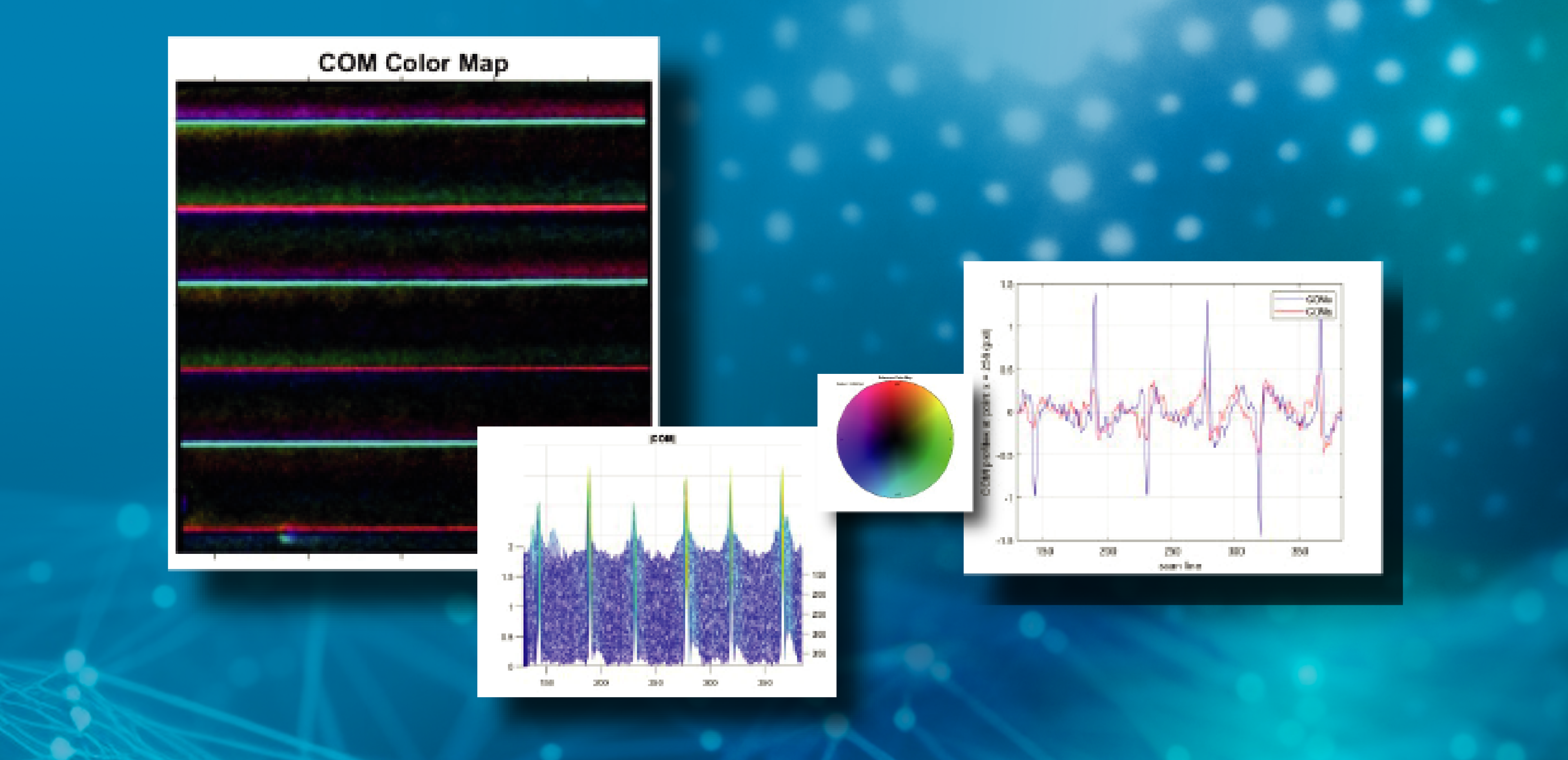
ELECTRIC-MAGNETIC
FIELD MAPPING
4D-SPED acquisition in combination with DigiSTAR and precession diffraction can be applied to characterize local electric or magnetic fields in materials ike transistors, sensors, nanowires, batteries etc. by detecting shift of the intensity distribution of the transmited central electron beam.

APPLICATIONS


NEWS
Special issue in MDPI
Symmetry for Electron Diffraction and Structrural Imaging I & II
MDPI special issues include a total of 19 published papers including contributions from important researchers in the field of electron crystallography and from leading Electron Diffraction device Manufacturers.
Dr. Partha Pratim Das, Dr. Arturo Ponce-Pedraza,
Dr. Enrico Mugnaioli, Dr. Stavros Nicolopoulos
Symmetry | Special Issue: Electron Diffraction and Structural Imaging I (mdpi.com)
Symmetry | Special Issue: Electron Diffraction and Structural Imaging II (mdpi.com)

EVENTS